-
Thermal Camera Core
-
Thermal Security Camera
-
Drone Thermal Camera
-
Plug-in Thermal Camera
-
Cooled Infrared Detectors
-
Cooled Camera Modules
-
Optical Gas Imaging
-
Infrared Thermal Camera Module
-
High Resolution Thermal Camera Module
-
Thermal Camera For Fever Detection
-
Vehicle Mounted Thermal Camera
-
Integrated Dewar Cooler Assembly
-
Uncooled Infrared Detectors
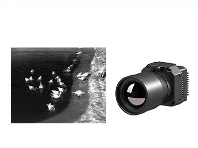
VOx High Resolution Thermal Camera Module Uncooled LWIR 1280x1024 / 12μm
| Resolution | 1280x1024/12μm | NETD | <50mK |
|---|---|---|---|
| Spectral Range | 8~14μm | Size | 20x20x10.4mm |
| Highlight | VOx Thermal Camera Module 12um,LWIR Thermal Camera Module 1280x1024,VOx LWIR Camera Module |
||
VOx Uncooled LWIR 1280x1024 / 12μm Thermal Camera Module for Industrial Temperature Measurement
PLUG1212R is one of the PLUG-R series uncooled infrared camera module developed by SensorMicro. It adopts the market preferred focal plane array VOx microbolometer uncooled infrared detector, professional signal processing circuit and image processing platform, completely transforms the target infrared radiation into temperature data. Its temperature measurement is available and temperature range can be customizable raging from -20℃~150 ℃ for industrial temperature measurement.
With large array 1280x1024 resolution, the PLUG1212R uncooled thermal module could present more image details and supports larger field of view. The reduced 12µm pixel size offer better spatial resolution and match shorter optical lens focus to achieve the same range mission.
- Pixel pitch: 12μm
- Resolution: 1280x1024
- Spectra Range: 8μm -14μm
- High Sensitivity: NETD<30mK
- Temperature Range: -20℃~150℃, 100℃~550℃
- Temperature Accuracy: ±2℃ or ±2%
- High reliability & Strong Environmental Adaptability.
| Model | PLUG1212R |
| IR Detector Performance | |
| Resolution | 1280x1024 |
| Pixel Pitch | 12μm |
| Spectral Range | 8~14μm |
| NETD | <30mk |
| Image Processing | |
| Frame Rate | 25Hz |
| Start-up Time | <25s |
| Analog Video | / |
| Digital Video | HDMI/RAW/YUV/BT1120 |
| Extension Component | USB/Camerlink |
| Dimming Mode | Linear/Histogram/Mixed |
| Digital Zoom | 1~8X Continual Zoom, Step Size 1/8 |
| Image Display | Black Hot/White Hot/Pseudo Color |
| Image Direction | Horizontally/Vertically/Diagonally Flip |
| Image Algorithm | NUC/AGC/IDE |
| Electrical Specification | |
| Standard External Interface | 50pin_HRS Interface |
| Communication Mode | RS232-TTL, 115200bps |
| Supply Voltage | 5±0.5V |
| Temperature Measurement | |
| Operating Temperature Range | -10°C~50°C |
| Temperature Range | -20°C~150°C, 100°C~550°C |
| Temperature Accuracy | ±2°C or ±2% (Take the Maximum Value) |
| SDK | ARM/Windows/Linux SDK, Full Screen Thermography |
| Physical Characteristics | |
| Dimension (mm) | 56x56x40.2 |
| Weight | ≤200g |
| Environmental Adaptation | |
| Operation Temperature | -40°C ~ +70°C |
| Storage Temperature | -45°C ~ +85°C |
| Humidity | 5%~95%, Non-condensing |
| Vibration | Random Vibration 5.35grms, 3 Axis |
| Shock | Half-sine Wave, 40g/11ms, 3 Axis 6 Direction |
| Optics | |
| Optional Lens | Fixed Focus Athermal: 19mm/25mm |
The PLU1212R infrared imaging module is widely used in Power Electricity, Machine Vision, Building Inspection, Metallurgical Petrochemical etc.
![]()
![]()
1. About ceramic packaging infrared detector
Ceramic packaging process is similar to metal packaging, which is a mature infrared detector packaging technology. Compared with metal packaging, the volume and weight of the packaged detector will be greatly reduced. For ceramic packaging, its readout circuit has self-adjusting operating temperature function and does not require TEC stabilization.
2. Wafer Level Packaging
Wafer-level packaging, also known as wafer-level size packaging, has become an important part of advanced packaging technology in the semiconductor industry. Wafer level packaging (WLP) is the process of completing high vacuum packaging directly on the entire MEMS wafer, then scribing and cutting to make a single infrared detector. It performs most or all of the packaging and testing procedures directly on the IR detector wafer before dicing.
It is an improved chip size package that meets the needs of small size, lightweight, portable, handheld, low price and high production efficiency.


