


All Products
-
Thermal Camera Core
-
Thermal Security Camera
-
Drone Thermal Camera
-
Plug-in Thermal Camera
-
Cooled Infrared Detectors
-
Cooled Camera Modules
-
Optical Gas Imaging
-
Infrared Thermal Camera Module
-
High Resolution Thermal Camera Module
-
Thermal Camera For Fever Detection
-
Vehicle Mounted Thermal Camera
-
Integrated Dewar Cooler Assembly
-
Uncooled Infrared Detectors
Contact Person :
Wendy Wang
Phone Number :
+86 27 50185150
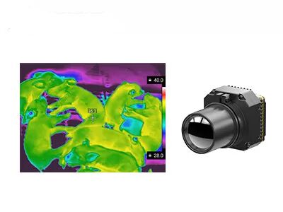
Clear Image Infrared Thermal Camera Module Core 640x512/17μm for ADAS

| Place of Origin | Wuhan, Hubei Province, China |
|---|---|
| Brand Name | SensorMicro |
| Certification | ISO9001:2015; RoHS; Reach |
| Model Number | PLUG617R |
| Minimum Order Quantity | 1 Piece |
| Price | Negotiable |
| Payment Terms | L/C,T/T |
Product Details
| Temperature Range | -20℃~+550℃ (Customizable) | Temperature Accuracy | ±2℃ Or ±2% |
|---|---|---|---|
| Resolution | 640x512/17μm | NETD | <30mK |
| Spectral Range | 8~14μm LW | Size | 44.5x44.5x36.6mm |
| Highlight | Clear Image Camera Module Core,17uM Camera Module Core,640x512 Camera Module |
||
Product Description
PLUG617R Uncooled Thermal Core
Infrared Thermal Camera Module Core 640x512/17μm for Industrial Thermography
Product Description
PLUG617R uncooled thermal camera module consists of 640x512 / 17μm uncooled fpa infrared detector, full series of optical components, professional signal processing circuit and image processing algorithm.
PLUG617R is a kind of uncooled camera module applied in the field of industrial thermal imaging and temperature measurement. The temperature range is customizable, which can meet the specific requirements of industrial thermography and present a clear thermal image.
As a leading thermal camera module manufacturers, SensorMicro is committed to opening a new vision for industrial temperature measurement. After years of technical accumulation and practical experience in the field of infrared temperature measurement, we have provided our customers a full range of machine thermal imaging vision solutions.
Main Features
- NETD<30mk, High Sensitivity
- Stable Performance
- Easy Integration
- Clear Image Quality & Details
- Customizable Temperature Range
- Strong Environmental Adaptability
Product Specifications
| Model | PLUG617R |
| IR Detector Performance | |
| Resolution | 640x512 |
| Pixel Pitch | 17μm |
| Spectral Range | 8~14μm |
| NETD | <30mk |
| Image Processing | |
| Frame Rate | 25Hz/30Hz |
| Start-up Time | <15s |
| Analog Video | PAL/NTSC |
| Digital Video | RAW/YUV/BT656/LVDS |
| Extension Component | USB/Camerlink |
| Dimming Mode | Linear/Histogram/Mixed |
| Digital Zoom | 1~8X Continual Zoom, Step Size 1/8 |
| Image Display | Black Hot/White Hot/Pseudo Color |
| Image Direction | Horizontally/Vertically/Diagonally Flip |
| Image Algorithm | NUC/AGC/IDE |
| Electrical Specification | |
| Standard External Interface | 50pin_HRS Interface |
| Communication Mode | RS232-TTL, 115200bps |
| Supply Voltage | 4~6V |
| Temperature Measurement | |
| Operating Temperature Range | -10°C~50°C |
| Temperature Range | -20°C~150°C, 100°C~550°C |
| Temperature Accuracy | ±2°C or ±2% (Take the Maximum Value) |
| SDK | ARM/Windows/Linux SDK, Full Screen Thermography |
| Physical Characteristics | |
| Dimension (mm) | 44.5x44.5x36.6 |
| Weight | <90g |
| Environmental Adaptation | |
| Operation Temperature | -40°C ~ +70°C |
| Storage Temperature | -45°C ~ +85°C |
| Humidity | 5%~95%, Non-condensing |
| Vibration | Random Vibration 5.35grms, 3 Axis |
| Shock | Half-sine Wave, 40g/11ms, 3 Axis 6 Direction |
| Optics | |
| Optional Lens | Fixed Focus Athermal: 7.5mm/13mm/19mm/25mm/35mm Motorized Lens: 75mm/100mm/150mm |
Industrial Applications
The PLUG617R thermal imaging module is widely used in Electric Power Inspection, Machine Vision, Building HVAC Security & Monitoring, Outdoors, Firefighting & Rescue, Law Enforcement & Rescue, ADAS, UAV Payloads etc.
![]()
About SensorMicro
SensorMicro was founded with a simple but powerful belief: Innovation should serve real-world needs.
SensorMicro exists to empower people and systems to see beyond the surface—into the patterns, the problems, and the possibilities that lie beneath.
By turning invisible heat into visible truth, we help industries make smarter decisions, protect what matters most, and navigate complexity with clarity.
Heeding to our insistence on being self-made and customer-first has become a sure recipe for SensorMicro's momentum. As our business spans much of the globe, we've charged ahead on all fronts—from security, firefighting, industrial inspection, medical care, and machine vision, to environmental monitoring and key aspects of carbon neutrality—helping partners unlock the full potential of intelligent infrared sensing, and connecting the dots of life.
We are more than an infrared technology company. We are a community of people committed to building a sustainable, ethical, and human-centered future. Every pixel of innovation we create is a promise — a promise to protect, to empower, and to serve.
FAQs
1. About ceramic packaging infrared detector
Ceramic packaging process is similar to metal packaging, which is a mature infrared detector packaging technology. Compared with metal packaging, the volume and weight of the packaged detector will be greatly reduced. For ceramic packaging, its readout circuit has self-adjusting operating temperature function and does not require TEC stabilization.
2. Wafer Level Packaging
Wafer-level packaging, also known as wafer-level size packaging, has become an important part of advanced packaging technology in the semiconductor industry. Wafer level packaging (WLP) is the process of completing high vacuum packaging directly on the entire MEMS wafer, then scribing and cutting to make a single infrared detector. It performs most or all of the packaging and testing procedures directly on the IR detector wafer before dicing.
It is an improved chip size package that meets the needs of small size, lightweight, portable, handheld, low price and high production efficiency.
Recommended Products